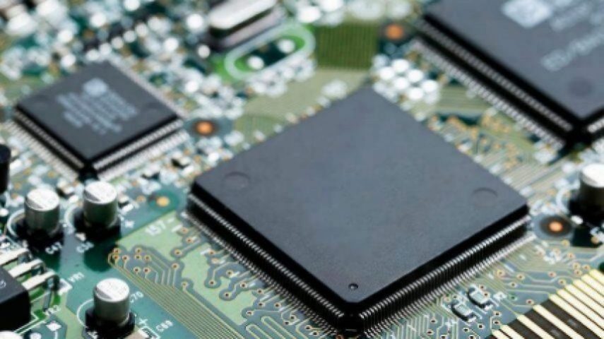
Mentor Boosts AI Chips with AI
Article By : Junko Yoshida
Mentor is all about Artificial Intelligence as the EDA industry heads into its annual Design Automation Conference.
On the brink of the Design Automation Conference (DAC), EDA companies are busy sharpening their message for the industry’s biggest annual conference. For Mentor, a Siemens business, this year is all about Artificial Intelligence.

In an interview with EE Times, Joe Sawicki, executive vice president of the Mentor IC EDA group at Siemens, said that the industry is surprised at the swift progress of fundamental AI research in universities. Even more surprising is that in the span of just a few years, these advances have spread and become almost ubiquitous throughout the commercial market. The improvements in AI are across almost all categories of the technology, from neural networks to machine learning (ML) to deep learning and inferences. For EDA companies, it has become imperative “to meet the growing needs by IC designers exploring various AI architectures,” Sawicki noted.
Asked about EDA’s role in AI, Sawicki claimed that “EDA tools can improve the levels and performance of AI” to a point previously not available.
Second, AI and machine learning are already used in full-chip manufacturing databases. AI/ML-powered Calibre tools are good examples. Already commercially available, Calibre Machine Learning OPC, for example, optimizes optical proximity correction. Calibre LFD with Machine Learning is deployed for advanced lithography simulation, according to Mentor.
Mentor, citing Samsung Electronics as a customer for its Calibre tools, noted Samsung’s foundry technology team used the new Calibre LDF with Machine Learning to improve accuracy by 25 percent when compared with Mentor’s earlier Calibre LDF solutions.
Third on Sawicki’s list is Mentor’s expanding portfolio of AI/ML-enhanced EDA tools. Last year, Mentor acquired Solido. The deal launched Mentor’s AI trajectory, adding a lot of AI expertise and customers. Solido’s customers – which Mentor claims include 15 of the world’s 20 largest global chip design firms – are using machine learning to “reduce the number of simulations, and significantly improve the yield,” explained Sawicki.
Explosion of architecture
As AI-based architecture has exploded, so too has its enabling tools. Designers of AI chips for edge devices, for example, need to explore many factors – including architectural complexity, power budgeting and high-speed IO. Many AI accelerators definitely demand much computational power than previously anticipated.
Ellie Burns, marketing director, digital design implementation solutions for Mentor, told us, “None of the AI chips available today – regardless if it’s a GPU for training, or a generic Tensor Processing Unit – would be able to fit the bill” for specific AI acceleration needs. CPUs/GPUs would use up way too much power, she said. Even generic ML accelerators lack the massive computational power and parallelism necessary to run certain real-time AI applications. In fetching some data and instructions from memory, CPUs always consume too much power, she added.
Facing such problems, designers start thinking about building their own AI accelerators. For that, they need tools for “architectural exploration,” Burns explained. This is where high-level synthesis (HLS) comes in, she added.
HLS programmed in C/C++, for example, makes architectural exploration much easier. HLS plays a critical role for designers to “get AI right, especially around memory.”

In Mentor’s opinion, HLS “enables the fastest path to build optimized AI/ML accelerators for edge applications.”
Today, there is no single right answer for AI accelerators. Designers in different fields are all looking for a specific design for their own AI accelerator applications. Some accelerators might employ strategies such as optimized memory use, and the use of lower precision arithmetic to accelerate calculation and bump up computation throughput.
Google’s TPU, for example, is specifically designed for a TensorFlow framework, which is extensively used for convolutional neural networks (CNN). It focuses on a high volume of 8-bit precision arithmetic. But depending on a specific neural network or a class of network, an entirely different strategy is feasible. A designer could use half-precision and the 16-bit floating-point format for AI acceleration.
Mentor’s new Catapult HLS AI toolkit, Mentor explained, delivers a few essential elements for AI acceleration design. It offers an FPGA demonstrator, so that designers can test new algorithms. Catapult HLS also offers “an object detection reference design and IP to help designers quickly find optimal power, performance and area implementations for neural network accelerator engines.” The company stressed that this is a task previously “not possible with hand-coded register transfer level (RTL) designs.”
Customers?
In its press release, Mentor identified Chips&Media, an AI silicon company based in Korea, as a customer for Catapult HLS technology. The Korean company is incorporating deep neural networks in its video and computer vision IP cores.
Earlier this year, Mentor also disclosed that Graphcore, an AI acceleration chip startup billed as the only Western semiconductor “unicorn,” is using Mentor’s EDA technology. Graphcore used Mentor’s design-for-test (DFT) and silicon bring-up tools called Tessent to deliver Graphcore’s Colossus Intelligence Processing Unit (IPU).
Laurie Balch, Research Director at Pedestal Research, when asked about AI-enhanced EDA tools, told us, “We are still in a very early implementation phase” – especially using AI/ML in “tools across the spectrum.” Noting that there is a natural connection between AI and EDA tools, she observed that everybody in the EDA industry is pumping resources into AI.