Design Centers in India: Unwinding Basic Considerations
Article By : Majeed Ahmad Kamran, EE Times India

Here is how design centers in India are evolving to reflect changes in the larger semiconductor industry while still being much of the same.
The design centers in India are going through a makeover of sorts at a time of an upheaval in the larger semiconductor industry. Especially, after a few failed attempts to set up a fab on the Indian soil.
And that merits a closer examination of the current state of design in India and answers to a few pertinent questions. For example, where does India's design landscape stand while chip industry is going through an unprecedented consolidation wave? Will pressure margins on the semiconductor business bring more design outsourcing work to India?
Will Indian design houses be able to contribute work related to the new chip architectures, another key motive behind semiconductor firms' quest to consolidate and move beyond the legacy architectures while innovating design solutions for new markets like ADAS and augmented reality?
Hanish Bhatia, senior analyst for Devices and Analytics at Counterpoint Research, says that design houses in India will continue to act as a support system of both IDMs and fabless semiconductor firms while mostly being restricted to low-end chip design work. "That's primarily due to lack of skilled workforce, such as EDA engineers, and competitive IC fabrication capabilities."
Take, for instance, mobile phone manufacturing in India, currently being dominated by the Chinese ODMs. Here, India is trying to identify gaps in terms of developing the skillset for full-scale smartphone design and manufacturing. "There is a need for a push to increase investments in relevant training programs at the grassroots level for appropriate skillset development," Bhatia added.
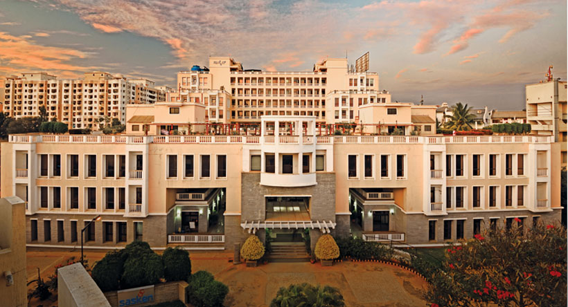
He also mentioned Sasken Technologies that now provides cognition R&D services for chipmakers like Intel. Bhatia said that Sasken's operations in Bangalore are primarily restricted to software-level support. "Indian design houses are catering to a small portion of a big opportunity."
Sasken's design center in Bangalore is focusing on low-power technologies like sensors, connectivity, and tracking solutions.
 Sasken's design center in Bangalore is focusing on low-power technologies like sensors, connectivity, and tracking solutions.
However, this small design pie in the larger semiconductor industry value chain keeps on growing. Sondrel, the UK-based concept-to-silicon design consultancy, is a case in point. It has recently acquired a design center in Hyderabad that formerly worked for Imagination Technologies.
The design center specializes in graphics and image processing, and now Sondrel aims to use it for large and complex digital designs for compute-intensive applications like artificial reality, machine vision, and deep learning.
Sondrel's CEO Graham Curren said that design, verification and implementation engineers at this center in Hitech City, Madhapur district, will help create ADAS, augmented reality and virtual reality solutions.
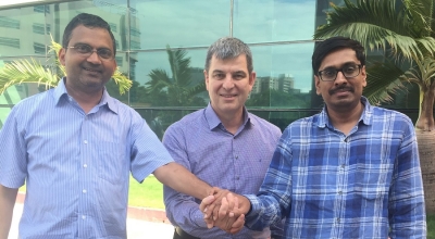
Sondrel's VP of Engineering, Kevin Steptoe, joined by engineers Hari Vattikota (left) and Ravikumar Dasari (right) at the company's Hyderabad design center.
 Sondrel's VP of Engineering, Kevin Steptoe, joined by engineers Hari Vattikota (left) and Ravikumar Dasari (right) at the company's Hyderabad design center.
The intellectual property (IP) products and services also mark a prominent opportunity for India's design houses amid the development of bigger and more powerful system-on-chips (SoCs). Especially, the smartphone industry offers a huge potential, as Bhatia pointed out while quoting the Indo-Chinese design venture Borqs.
The company's design house in Bangalore, a license holder from Qualcomm, is optimizing the speaker capabilities for low-end mobile devices by cutting down noise and filtering out background sounds. "However, such firms are always under the radar for getting acquired as bigger players aspire in-house capabilities and inorganic growth," Bhatia said.
And that brings us to a key shift in India's design landscape mainly encompassing chip design, board design, and embedded software development. The multinational firms like Cadence and Qualcomm as well as local outfits such as Wipro and Infosys have been acquiring smaller chip design firms during the past couple of years.
These acquisitions are largely being made for staff augmentation and business model adjustment. But the end goal looks somewhat common: How to best serve tier 1 to tier 3 semiconductor customers.
"And, as the market matures, we can expect Indian firms to develop more research-intensive capabilities through training programs," Bhatia concluded. "As of now, India is at least a decade away from developing core architecture design capabilities."
Majeed Ahmad is former editor-in-chief of EE Times Asia.