Hot Chips 2019: The Hottest and Biggest Yet
Article By : Kevin Krewell
While Cerebras is building the largest chip ever, other vendors are looking to see how they can disaggregate the larger dies.
There were two keynotes at this year’s Hot Chips conference, one given by AMD’s CEO, Lisa Su, and the other by TSMC’s Research VP, Philip Wong. Both touched on Moore’s Law, but while Su talked about how applications need to go beyond Moore’s Law, TSMC’s Wong committed that Moore’s Law is not dead (for transistor density, at least). Su contended that leading-edge silicon costs continue to increase, which is why AMD transitioned to its chiplet strategy. The TSMC presenter didn’t talk cost, but did offer many forms of multi-die packaging solutions, seemingly re-enforcing Su’s assertions.
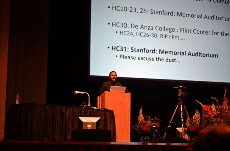
Hot Chips is held every August, and this year it opened with a record crowd in Memorial Auditorium at Stanford University. Approximately 1,200 people attended the event, which stressed the capacity of the Stanford venue. It is difficult to determine what drove the larger audience: the merit of the materials, better recognition of the event, better promotion, or the bubble in money flowing into machine learning chips these days. Machine learning was certainly a major theme of this year’s Hot Chips event; half of the presentations were related to machine learning and neural network processing.
Recommended
EE Times on Air: Startup Spins Whole Wafer for AI
Cerebras: Wafer-scale die
The presentation that garnered the most attention was the introduction of a wafer-scale machine learning processor from Cerebras. This was the first detailed disclosure by the company since it was founded and the presentation just scratched the surface of the technologies that are required to build a wafer scale size die. The session chair’s introduction was quite appropriate, this was the hottest chip ever introduced at Hot Chips (although not disclosed in the presentation, it has been reported that the chip dissipates 15 kW of power). The scale of the chip is hard to imagine when the die sides are about 8.5 inches. The company certainly has expanded our concept of what it means to build a “big” chip.
Nvidia: ‘Compute tile’ die in a package
While Cerebras is building the largest chip ever to make it into production, other vendors are looking to see how they can disaggregate the larger dies they are building today. Probably the biggest contrast was the project from Nvidia Research. Nvidia Research’s RC18 test chip was designed for scalable deep learning inference using 36 “compute tile” dies in a package. Each 16nm compute tile is capable of 9.5 TOPS/W, for 128 TOPS total. A high-speed interconnect using Ground Reference Signaling (GRS) 100 Gbps per link with multicast capability and a token-based chip-to-chip protocol connects the die in the package. Fewer than ten researchers took the chip from specification to tapeout in 6 months by using high-level abstraction (C++) automated design and agile design to show that a small team can produce a fast time-to-market solution.
MCP & Chiplet
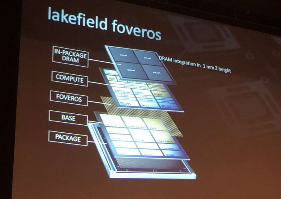
Multichip packaging and chiplet technology made its presence felt throughout the conference, with related products and technologies from AMD, Intel, Nvidia, and TSMC. Intel demonstrated a way to pack a full Lakefield PC platform (processor and memory) into extremely compact package using die stacking technology called Foveros. Lakefield also has a heterogeneous processor configuration with one big x86 CPU core and four smaller Atom cores in one die. The 10nm+ Lakefield processor die has very low standby power and uses a PMIC for power management. Charts showed peak power of around 7W when running graphics-intensive workloads.
Benchmarking
Another interesting presentation focused upon the nascent benchmarking of machine learning chips. The industry consortium behind MLPerf gave a presentation on its latest efforts to benchmark machine learning training. That consortium includes a number of the heavy hitters, including Arm, Intel, Facebook, Google, Nvidia, and Xilinx. Even though the specification is still in its early stages, several vendors are already publishing preliminary numbers. Unfortunately, the benchmark for machine learning inference is not yet complete. In addition, MLPerf doesn’t have benchmarks for the tougher sparse data applications.
Sparse data is a particular problem for Facebook, which talked about its Zion platform for ML training. What was interesting is that Facebook has unified its CPU and accelerators training platform to use the new BFLOAT16 data format (BFLOAT16 is based on the IEEE 32-bit floating point format with the mantissa truncated to only 7 bits).
Habana, Huawei, Intel and Xilinx
Additional machine learning and neural net chips were presented by Habana, Huawei, Intel, and Xilinx. Huawei detailed its DaVinci neural network (NN) accelerator. The DaVinci design is particularly unique because it was designed to scale from IoT devices to data centers. The company is committed to incorporating the NN processor into its diverse chip designs. The presentation was also unique because the presenter was denied a visa to the U.S.A., so Huawei prepared a high-quality video of the presentation and the presenter took questions over a conference call after the presentation.
Recommended
Huawei Paints Broad AI Canvas
Intel presented its Spring Crest (NNP-T) ML training chip and the NNP-I inference engine. The NNP-T part is based on the Nervana chip architecture, now ported to TSMC’s 16nm process. The 27 billion transistors chip is 680mm2, on a 1200mm2 interposer with 32GB of HBM2-2400 memory. The chip is designed to fit into Facebook’s Open Accelerator Module (OAM) form factor, and it supports the BFLOAT16 data format.
The other Intel NN chip is the Intel NNP-I Spring Hill inference chip that will be available in an M.2 PCIe form factor. It’s targeting best-in-class perf/power efficiency for major data center inference workloads at 4.8 TOPs/W. Spring Hill is being built in Intel’s 10nm process.
Habana gave an update on the company’s Goya inference card introduced last year and the Gaudi training board that is in evaluation. Like Intel’s Spring Crest, the Gaudi training chip has support for the BFLOAT16 data format and is also provides it in the Open Compute Project (OCP) OAM. Gaudi’s chip-to-chip interconnect is standard RDMA RoCE over PCIe 4.0.
Xilinx’s 7nm Versal VC1902 “ACAP” chip has 37 billion transistors and approximately 1GB of on-chip memory. Versal was introduced in 2018 and is now in evaluation samples.
Despite the wave of machine learning and neural net processors at Hot Chips, there were also some more traditional presentations including AMD’s Zen 2 (Matisse processor) and Navi GPU, Arm’s N1 server core, IBM’s POWER 9 AIO, Intel’s Lakefield PC processor, Nvidia’s Turing GPU with ray tracing acceleration.
Silicon disaggregation was also a key part of the IBM Power 9 AIO with the Open Memory Interface, which offers a way to remove the memory controllers from the processor die and put them into the memory module. The OMI logic is one sixth the area of DDR memory drivers and using OMI keeps the CPU chip memory agnostic. Microchip already has an OMI DDR4 memory buffer chip. IBM also made a case for its OpenCAPI accelerator interface and hinted that it was open to finding a path to converge with Intel’s CXL standard.
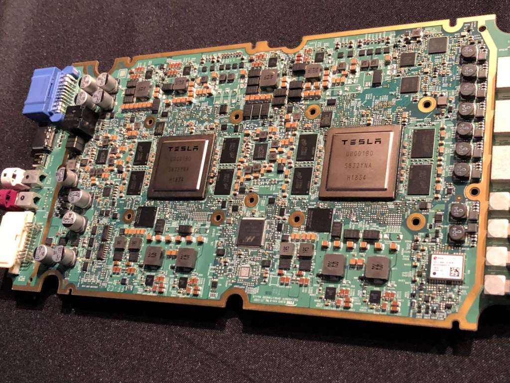
Hot Chips is a unique venue for companies to talk about chips they really would normally not talk about and any other conference. This was a case for Microsoft talking about the chip that goes into HoloLens 2 and Tesla talking about the custom ADAS chip it designed in-house for its cars.

While the material at Hot Chips can be quite technical and weighty, it’s not to say that people don’t have fun at the conference as well. This year Intel held a special after-show event nearby the Stanford campus where Raja Kaduri and Jim Keller were interviewed, while the same time eating progressively hotter hot wings. Intel certainly had a very large presence at this year’s hot chips as a sponsor and as a presenter, maybe in part, due to discontinuation of the Intel Developer Forum (IDF).
Hot chips conference is certainly a great venue to meet and talk to some of the leading minds in the chip industry. The conference is the best venue leading-edge trends in the processor industry and this year was no exception. If Hot Chips 2019 is any indication, the revolution in machine learning/artificial intelligence chips is alive and well.
— Kevin Krewell is Principal Analyst at TIRIAS Research.