Soitec Seek New Wafer Material
Article By : Junko Yoshida
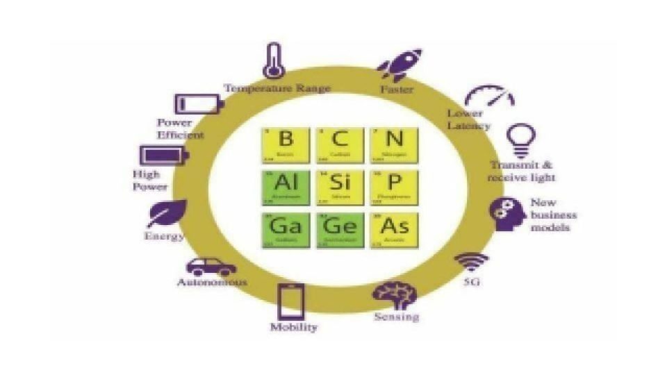
With 5G, the complexity of RF front-end modules is increasing at a bewildering pace. More antennas, more PAs, more filters are coming into modules, while each using different materials, beyond silicon, to improve quality.
BARCELONA – Despite the Mobile World Congress cancellation, the pursuit of 5G grows fiercer by the hour, especially among electronics players who are hitting silicon performance limits for 5G RF front-end modules.
Among the candidate materials to supplant silicon are compound materials such as gallium nitride (GaN), gallium arsenide (GaAs), and silicon carbide (SiC), along with piezoelectrics, which are being used to improve filters. GaAs has been used for power amplifiers in 4G and 5G handsets. GaN has begun gaining traction for power amplifiers in 5G mmWave markets.

More and more RF fabless chip companies are seeking “new materials to solve their problems,” Paul Boudre, CEO of Soitec, told EE Times this week in an interview here.
Together with CEA-Leti, Soitec (Grenoble, France) pioneered silicon-on-insulator (SOI) substrates. Already very successful with RF SOI wafers (used by RF chip companies to make switches and antenna tuners for smartphones), Soitec is poised to expand by branching into the new world of compound materials.
Boudre described a Soitec plan “to develop, generate and offer new materials based on our engineered substrates” for fabless chip companies. A list of Soitec’s new material adventures includes:
- Piezoelectric-on-insulator (POI) engineered substrates — used to produce high-performance surface acoustic wave (SAW) filter components for 4G and the 5G New Radio (NR) bands
- GaN-on-Si, GaN-on-SiC epiwafers. Soitec last year acquired Imect’s spinoff EpiGaN in Belgium, which developed the epiwafers. By integrating EpiGaN into Soitec and bankrolling the necessary tools, Soitec plans to enter the high-volume manufacturing base for the 5G GaN power amplifier market.
- Soitec will this year start sampling SiC wafers based on the company’s proprietary technology called Smart Cut.
Soitec’s Smart Cut process allows Soitec engineers to define materials, grow single-crystalline layers of those materials, and then transfer those layers from one substrate to another. This makes it possible to create active layers of a wafer that can be managed independently from the supporting mechanical substrates.
Soitec’s goal, applying Smart Cut to SiC, is to significantly improve SiC at the substrate and device levels both in cost and quality.
The bulk of Soitec’s products are based on FD-SOI and RF-SOI substrates, both of which leverage Smart Cut technology. Soitec, similarly by using Smart Cut, has also recently put POI into volume production. Next up are Smart Cut-based SiC wafers, scheduled for sampling later this year.
Why SiC?
But why SiC now? Even with a boom in demand, SiC faces two big challenges. First, there aren’t enough SiC wafers to go around. Second, when it comes to yield rate, SiC sucks.
Soitec has engineered new Smart Cut SiC wafers with these problems in mind, first by substantially improving the quality of the SiC layer on the substrate, and second by transitioning from current 6-inch SiC wafers to 8-inch wafers in order to reduce the cost. Soitec currently has a SiC-wafer pilot line in Grenoble.
To bolster its efforts, Soitec last fall announced a joint development program with Applied Materials. Applied joined with Soitec to get engaged in materials engineering innovations for silicon carbide technology.

Thomas Piliszczuk, Soitec’s executive vice-president of global strategy, cited two potentially large markets for Smart Cut-based SiC. One is for EV inverters, aiming for major battery-life improvements. Another is to capture “5G base-station demand for high-power efficiency and stringent linearity in power amplifiers.”
Given the shortage of SiC wafers on the market today, what’s Soitec’s business model? Boudre said, “It’s a good question. We can be SiC wafer providers ourselves, or we can partner with others by licensing.” Either way, he said, “Our goal is to reinforce SiC wafer supplies, improve its quality and transition it to 6-inch wafers. All of this will help make the cost structure of SiC wafers competitive.”
In search of new materials beyond silicon
RF semiconductor designers are scrambling for new materials and new designs/architecture for 5G systems. But why?
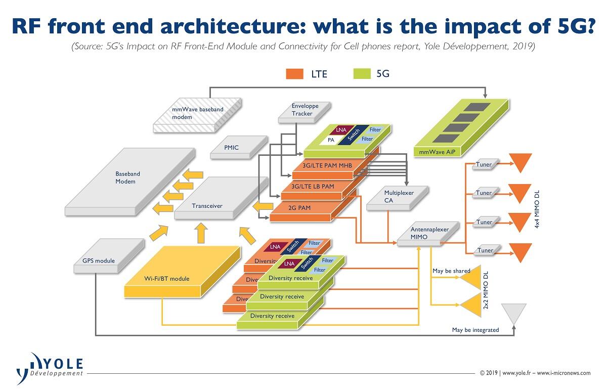
Because 5G uses more different high-frequency bands to enable high speed data transmission, the number of power amplifiers, filters, switches, LNA, antenna tuners that must go inside 5G RF front-end modules are multiplying at a bewildering rate. The sheer volume of parts and components — many remain discrete — is a headache for smartphone designers who must squeeze all those RF modules into a 5G phone.
5G smartphone developers are also worried about the quality, thermal dissipation and efficiency of RF components, because they could bog down RF front-end modules’ performance.
Moreover, not every RF component uses the same material or same technology. As noted, POI is used to improve filters. GaAs has been the leading material for power amplifiers (PA). But many PA suppliers today are taking a hard look at GaN. On another hand, RF SOI, a specialized SOI process, has become the standard for making such RF chips as switch devices and antenna tuners, for 3G, 4G and 5G smartphones and other products.
As Boudre explained, Soitec’s RF-SOI, available since 2016, has gained a lot of RF component customers. These customers opened Soitec’s eyes, because every RF fabless company is looking for new materials and substrates to build chips that meet the stringent requirements of 5G’s RF.
One example is power amplifiers for smartphones and base stations.
PA chips in 5G wireless applications are much different from those employed in 4G networks. Broadband modulation for 5G transmissions demands high-power efficiency and strict linearity from power amplifiers. Moreover, 5G networks will employ phased-array antennas to focus and steer multiple beams. With a 4×4 phased-array antenna, for example, the power amplifier must operate at much lower power than for the single-beam signals currently common in cellular systems.
The story gets even more complicated with a 5G network transmitting at millimeter wave (mmWave) frequencies. Compared to a sub-6GHz systems, a mmWave counterpart faces even more complicated RF design challenges.
Multiple-input multiple-output (MIMO) antennas are a 5G necessity, because they must serve many devices in densely deployed environments. They will require power amplifier chips with high-power efficiency and stringent linearity. Phased-array MIMO antennas with numerous RF front-end components will also ask for power amplifiers that offer greater integration at lower cost.
The strict requirements imposed by 5G handsets and base stations for power amplifiers led Soitec to aquire EpiGaN.
For both 5G infrastructure and handset architectures, mandatory attributes for RF semiconductor devices are “efficiency, compactness, low cost, high power density and linearity,” according to an article co-written by Markus Behet, Joff Derluyn, Stefan Degroote and Marianne Germain at Soitec’s GaN business unit. The article said, “Judged in terms of wideband performance, power density and efficiency, legacy technologies — essentially silicon LDMOS (laterally-diffused metal-oxide semiconductor) or GaAs — are no match for GaN HEMTs (High-electron-mobility transistor), regardless of whether they are grown on silicon or SiC.”
In the authors’ opinion, GaN technology is “meeting stringent thermal specifications for 5G, while preserving valuable PCB space for the tightly clustered massive MIMO antenna arrays. In base stations, discrete designs are already being replaced by space-saving multi-function GaN MMICs and multi-chip modules.”
What about Qualcomm?
Given the emergence of all these new materials — beyond silicon — supposedly to enable the integration of 5G mmWave RF front-end modules, what’s Qualcomm’s solution?
Qulacomm examined the available options, but in the end, the company chose silicon-based RF solutions, observed Claire Troadec, Power & Wireless Division director at Yole Développement.
Most likely this is because it was Qualcomm’s first-generation 5G mmWave RF front-end module, noted Boudre. He is confident that RF solutions leveraging GaN-on-Si technology, for example, could come into play, maybe in the company’s third or fourth generation of 5G RF modules.
GaN on SiC vs. GaN on Si
EpiGaN has developed both GaN-on-SiC and GaN-on-Si epiwafers.
What are the differences between the two?
Piliszczuk explained that both target the same market. “Today GaN on SiC has leadership” because it is more mature, he said. “Multiple device makers are working today on GaN-on-Si solutions also for handsets.”
In applications, GaN on SiC is used today for wireless infrastructure (4G/LTE base stations), defense, communication satellite applications “where highest performance and reliability is mandatory,” observed Piliszczuk. “GaN on SiC is also a strong contender for 5G MIMO infrastructure,” he added.
Piliszczuk acknowledged that GaN on Si has similar RF performance as GaN on SiC, but is less mature and has thermal constraints associated with the use of the silicon substrate.
But Soitec is bullish on GaN on Si, because presumably, it can take advantage of the significant economies of scale inherent in silicon processing. Piliszczuk believes it can “open up new high-volume and consumer markets.” According to Soitec, 200mm GaN-on-Si products are available today from EpiGaN/Soitec. He noted that GaN-on-Si is also a strong contender for 5G infrastructure and handsets.
Yole Développement’s Antoine Bonnabel, technology and market analyst for RF devices and technologies within the Power & Wireless division, remains more cautious.
He told EE Times, “GaN on Si is not yet mature enough to be used commercially.” Meanwhile, “GaN on SiC is today used.” He explained that both approaches target the same application: power amplification for high frequencies.
According to Bonnabel, “The issue today is that GaN-on-SiC technologies are too expensive compared to silicon-based solutions. This is the case especially for low-power power amplifiers for massive MIMO, or for power amplifiers with less than 3 GHz frequencies. In addition, it cannot be integrated for small power applications like massive MIMO.”
In his opinion, “GaN on SiC is only used when no other solution exists, such as for high-power power amplification in frequencies over 3 GHz: typically 20W power amplifiers for band n77 – n79 currently in pilot / deployment phase.”
On the other hand, Bonnabel said, “GaN-on-Si solutions are not as good as GaN-on-SiC approaches, but they can potentially be lower cost.”
This means, he explained, that GaN on Si could compete on lower power amplification with Si-based LDMOS technology, thanks to a low-enough price and its integration capability (which GaN on SiC does not have).
Bonnabel concluded, “If Soitec or other players manage to manufacture good quality GaN on Si at reasonable prices, it could clearly compete with Silicon-based technology. And therefore, it will penetrate the lower power amplifiers market for massive MIMO. At the end, it could also replace GaN-on-SiC solutions for higher power applications.”
Asked about Soitec’s EpiGaN gambit, Yole’s analyst said, “Soitec has a long history in entering new innovative markets and managing to offer the best-in-class substrates. At Yole, we expect the company to do the same with GaN technologies.”
Future of alternative materials & structures
Researchers are looking ahead of the future where chip designers can leverage different materials in 3D integration. Earlier this month, Nadine Collaert, program director at Imec, discussed in a plenary session at the ISSC: “The industry is moving to higher frequencies and higher efficiency. One option is combining III-V materials (e.g. GaN and SiC) with CMOS to get the benefits of both materials.” She said, “That can be done with 3D integration,” showing several examples including an image of a 3D nano-ridge with a III-V material grown on a silicon-on-insulator (SOI) substrate. However, she cautioned, “There’s a lot of work that needs to go into enabling this.”
Soitec CEO Boudre, during the interview in Barcelona, noted that RF chip companies want a variety of options when it comes to technologies they can use to make their chips. Depending on the design and architecture of their RF front-end solutions, “We think it’s our job to offer to our customers a broad range of solutions a la carte — ranging from FD-SOI, RF-SOI to GaN and SiC.” In his mind, there will be opportunities to create a range of a new kind of engineered substrates.
“We think there will be a day when we can develop GaN-on-SiC on Si, for example. Why not?”