Modeling of Wide Band Gap Devices for Accurate Simulation
Article By : Balaji Siva Prasad Emandi
Creating accurate models for Wide Band Gap (WBG) power devices representing their complete behavior is vital to the system simulation for ensuring that the simulation results are highly accurate.
Creating accurate models for Wide Band Gap (WBG) power devices representing their complete behavior is vital to the system simulation for ensuring that the simulation results are highly accurate.
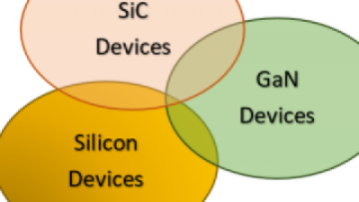
Wide Band Gap (WBG) devices such as Silicon Carbide (SiC) and Gallium Nitride (GaN) are becoming popular. Thanks to their promising features that surpass typical silicon devices and most importantly, the advances in manufacturability of these devices. The wide band gap of these devices allows for higher blocking voltage capabilities and their use in high voltage applications. These devices also exhibit lesser ON resistance and faster switching times. The devices have high thermal conductivity allowing for simpler heat management and can work at higher temperatures. Table 1 lists comparison of the key parameters between Silicon, SiC and GaN materials.
|
Material |
Band Gap (Eg) |
Thermal Conductivity (l) |
Electron Mobility (µ) |
Electron Saturation Velocity (Vsat) |
Breakdown Field (EC) |
|
Si |
1.12 |
1.5 |
1450 |
10 |
0.3 |
|
4H-SiC |
3.2 |
3.8 |
900 |
22 |
2.4 |
|
GaN |
3.39 |
1.3 |
2000 |
25 |
3.3 |
Units: Eg – eV, l – W/(cm.K), EC – MV/cm, µ – cm2/V.Sec Vsat – 106 cm/sec
Table 1: Physical Properties of Si, 4H-SiC and GaN Materials.
The wide band gap devices find their usage in applications that operate at higher voltage ranges, higher switching speeds and higher power control with reduced switching losses. An exponential growth in usage of the SiC and GaN devices is forecasted in the next few years, particularly in the fields of automotive and renewable power generation.
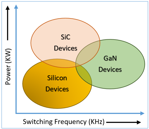
Figure 1: SiC and GaN devices’ market share
The higher switching frequencies and high voltage withstanding capabilities calls for revisited gate drivers and designs to curb the imminent Electromagnetic Interference (EMI). As engineers create designs for resolving these new requirements, productivity can be improved if the designs can be simulated and validated before going for a physical prototype.
Modeling and Simulation
Assimulation of the systems becomes an integral part of product design process the use of accurate models form the backbone to estimate the system’s performance precisely, which requires that the power devices are accompanied with models that emulate the device behavior comprehensively. Hence, creating accurate models for Wide Band Gap (WBG) power devices representing their complete behavior is vital to the system simulation for ensuring that the simulation results are highly accurate. Modeling complete behavior involves characterizing the component’s behavior for its:
- Normal operating conditions
- Performance at different temperatures
- Switching and other dynamic characteristics
- Statistical variations
- Safe operating area / stress limits
- Transient thermal characteristics
Most modeling solutions available today have limited flexibility and are not efficient in developing comprehensive models for the devices. Since SiC and GaN devices are used in advanced and complicated applications, having detailed models is crucial.
Modeling SiC and GaN MOSFETs
Asoutlined earlier, creating accurate models is the key to estimating the system’s behavior precisely. Advanced simulation tools, such as SaberRD, provide a solution for accurate modeling of Power MOSFETs (e.g. SiC and GaN). SaberRD allows design engineers to scan the graphs / characteristic curves directly from the datasheets and create a comprehensive model.
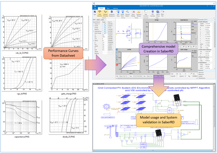
Figure 2: SaberRD’s Power MOSFET Tool flow
- The salient features of the SaberRD’s Power MOSFET Tool are:
- Characterizing accurate model from datasheet curves.
- Ability to model devices with different materials such as Si, SiC, GaN, etc.
- Intuitive user interface and advanced optimizing algorithms.
- Characterization of transient thermal network model, statistical variation, and stress limits in one tool.
- Inbuilt library of characterized components from major manufacturers of WBG devices such as CREE/Wolfspeed, EPC, etc.
- Simulate parasitic elements that can be imported from 3D modeling tools to estimate switching losses and EMI more accurately.
Summary
As the application of SiC and GaN devices increases, the need for accurate models is an immediate requirement. Modeling tools like Power MOSFET Tool in SaberRD can be leveraged to accurately model such devices and validate them in the system through simulation.
— Balaji Siva Prasad Emandi is a Corporate Application Engineer for Saber in the Verification Group at Synopsys. Balaji enthusiastically supports pre- and post-sales customers in the domain of simulation and development of Power Electronic subsystems.