ISSCC: Automotive Processors, Chiplets, and 5G
Article By : Kevin Krewell

AMD, MediaTek, TI, IBM, Samsung and CEA-Leti all made leaps in circuit design, which they discussed during the processor track at ISSCC.
SAN FRANCISCO — This year’s processor session at the ISSCC led off with two presentations by AMD (for the first time) followed by presentations from Samsung and MediaTek talking about their latest 5G smart phone chips, a research project/proof of concept design from CEA technology, an automotive system on chip (SoC) from Texas Instruments (TI), and the latest IBM Z series mainframe processor.
And because this conference is primarily a circuit design conference, each vendor focused on one or more specific aspects of circuit design that was unique in their processors.
The International Solid-State Circuit Conference (ISSCC) is one of the longest-running technical conferences in the semiconductor industry; it takes place every February here. The conference has a mix of academic and industry participants to discuss the latest challenges in chip circuit designs.
This year’s conference covered a deep vein of topics that included phase lock loops, low power circuits, memory, SerDes, DSP, and processor design. In particular, the processor section has the leading vendors appearing, but there are also projects from research institutes and academia. The sessions are jam-packed with dense chip design details. This is a highlight of the more interesting details from the processor session.
AMD Zen 2 and EPYC chiplets
Two AMD sessions dovetailed with each other with a discussion of the design of the Zen 2 CPU core used in the newest EPYC server processor, and a discussion of the EPYC chiplet architecture that allowed AMD to deliver 64-CPU cores in one socket without a massive die. The chiplet design also allowed AMD to apply three die designs to a plethora of products and markets.
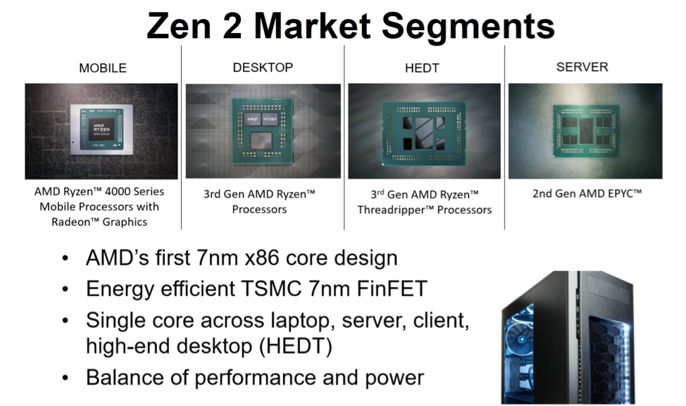
The AMD Zen 2 presentation described the challenges of making the first x86 processor using TSMC’s 7 nm process. The design goals for the EPYC server processor was to double the number of CPU cores within the same socket, without exceeding the socket power envelope. In addition, each CPU core was designed to give a 15% instructions-per-cycle performance uplift on the SPECint 2006 benchmark. Many of the architectural changes in Zen 2 have been discussed before. In the ISSCC talk, AMD focused on the circuit design challenges.
The AMD design is very modular. The basic element is the CPU Complex (CCX) with 4 CPU cores, L2 and L3 caches, and an Infinity Fabric system interconnect. With a 4-core module, AMD could scale the design from notebooks (4-8 cores) up to servers (with up to 64 cores). The CCX module was shrunk from 44 mm2 in the prior generation to 31.3 mm2 in Zen 2, despite adding more L3 cache.
The 7 nm process design required adding more metal levels. As a result, there were changes to the metal layer routing rules, and the design migrated from 10.5 tracks to 6 tracks. The lower track number offered challenges (less height and less drive strength) but had the benefit of lower leakage, reduced capacitance-per-cycle by 9% and produces a smaller die area.
AMD used a variety of design techniques such as clock shaping and had five different flip-flop designs, which were important for critical timing loops. The designers also moved more of the power budget to combinatorial logic by 3%, to get more performance. With these and other circuit optimizations, AMD could increase clock speed up to 4.7 GHz and lower the operating voltage when run at clock speed comparable to the original Zen core.
The second AMD presentation described the changes in AMD’s chiplet strategy for Zen 2-based server products. One of the key benefits for AMD was that with just three die tape outs, AMD could build products to support multiple markets. There were also thermal benefits to using chiplets as the chips were spread out across the package.
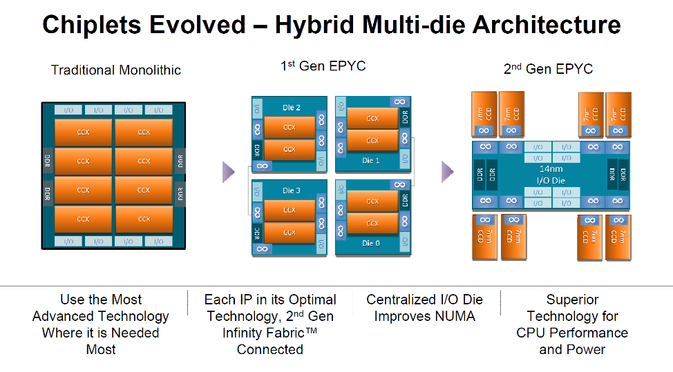
AMD’s goal was to deliver substantially more performance per socket and the result was double the number of CPU cores in the second-generation EPYC processor. This puts AMD on track to double performance every 2.5 years (SPECint 2006). The new EPYC processor also achieved improved memory latency. Using chiplets let AMD build server chips that were not feasible nor economical in a monolithic chip as it would have hit reticle limits to get to 64 cores.
AMD also optimized the cost structure and improved die yields by using much smaller chiplets. AMD used the expensive 7 nm process for the Core Cache die (CCD) and moved the DRAM and PCIe logic to a 12 nm I/O die fabricated by GlobalFoundries. Each CCD is composed of two CCX modules with four Zen 2 cores and the L2 and L3 caches, where 86% of the CCX is dedicated to CPUs and L3 cache. Each CCD still needs to be a mini SoC that includes power management, Infinity Fabric system interconnect, clocks, etc., on die.
With all these requirements, there were many challenges. With the memory controller now centralized on a separate chip for all CCX modules, the new EPYC processor could achieve improved average memory latency. But, the best-case latency still required going off the CCD to access memory. As a result, the AMD design focused on reducing the Infinity Fabric latency, so the best-case latency was only 4 nanoseconds longer.
Because AMD committed to keeping the EPYC package size and pinout unchanged, there needed to be a close silicon/package co-design as the number of die increased from four in the first EPYC to nine in the second-generation EPYC. The routing paths were very tight and required routing signals under inner CCD chiplets to reach CCD chiplets further away from the centralized I/O die.
Many of the other ISSCC talks featured the circuits that compensate for internal voltage dips (droop) when the processors are under heavy load. AMD has a current shunt — extra current — to fight droop and can also stretch clocks. The same low dropout (LDO) design allowed individual core linear regulation that enables power savings by adapting the voltage to each core’s capability.
Proof-of-Concept Processor has 96 cores and an Active Interposer
The one non-production chip in the session was a 96-core processor that used the chiplets strategy as well, but while AMD used a multi-chip module with a dedicated I/O die, this chip used an active silicon interposer that put the I/O logic into the interposer.
The design gets up to 220 GOPS out of 96 cores using six chiplets. It was designed by CEA-Leti and fabricated by ST Micro. The idea here is to prove this concept using two die designs — the chiplet and the active interposer. While this design uses homogeneous chiplets, a future design could use heterogeneous processing elements. As with the AMD EPYC design, the CEA’s goals are to add more processing elements, where a single die is insufficient to deliver the required processing. One such application could be autonomous vehicles, where many hundreds of GOPS will be required.
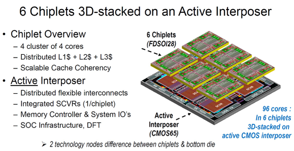
With an active interposer, many functions that can run in older process nodes can be offloaded from the processing elements. Those include power management, memory interfaces, and I/O. For this particular design, CEA used distributed interconnects with a 2D-mesh. The interconnects on the interposer used a mix of passive channels for short distances and active for longer connections. The design also used a novel asynchronous QDI logic for communication with an asynchronous network on chip router.
The processing element chiplet was fabricated using FDSOI 28 nm LPLV with body bias and the active interposer used 65 nm. While this chip used older process nodes, the goal was to show how it could be built and manufactured. The chiplets were tested using traditional known-good-die techniques, but the active interposer was only tested once all the elements were assembled. In full production, with more advanced process nodes, that manufacturing flow will likely be different.
Samsung and MediaTek 7 nm 5G smartphone chips
The two 5G smartphone SOC designs, one each from MediaTek and Samsung, focused on the CPU design issues of mixing different Arm cores for the big.LITTLE architecture. In addition, both addressed the issue of internal voltage droop detection when processing units are under heavy load.
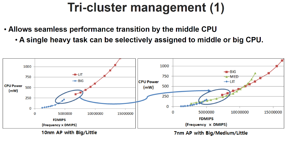
The first presentation was from Samsung. The company chose to build a tri-cluster set of CPU cores, rather than the dual-cluster from Arm’s big.LITTLE. Samsung used Arm-licensed cores for two of the three clusters, but the highest performing cores were designed by Samsung itself under an architecture license from Arm — the two M4 cores. The dual M4 cores have a separate 3 MB L3 cache and the core target Intel i5 level of performance.
For the middle power/performance range, Samsung used Arm Cortex-A75 cores. The “little” power-efficient cores were venerable Cortex-A55. The gap in power/performance between the Samsung M4 cores and the Cortex-A55 cores was too great and Samsung added the Cortex-A75 cores to bridge the gap. Samsung also added a neural processing unit with 1,024 MACs, but it didn’t provide a lot of detail.
Voltage drops in high-performance processors can be a problem. If you add too much guard band, by keeping the supply voltage higher, you burn more power. At a more power-efficient nominal voltage, when a particular power-hungry unit is under load — such as a GPU running a high-resolution game — the internal resistance drop can cause the internal voltage to drop below specification. SOC vendors build in specialized circuits to detect these voltage drops and take action to mitigate the problem. Their approach is to stretch out the clock to slow the circuit and reduce power consumption by effectively lowering the clock speed. Samsung uses a ring oscillator circuit that changes speed depending on the voltage. If the oscillator runs a counter that is compared with a threshold. Droop detection sets a flag in the clock management unit (CMU) and halves the clock speed.
MediaTek takes a different approach to CPU core selection by sticking to the Arm big.LITTLE scheme, which MediaTek called a dual-gear design. MediaTek uses the newer Cortex-A77 CPU cores for the big performance cores. MediaTek also noted that the Cortex-A55 little cores are not keeping pace with developments in the performance cores. Instead of adding mid-performance cores, they worked to extend the voltage range for the A77 to lower speeds. While Samsung had only two performance cores, MediaTek has four of the A77 cores. The four A77 and the four A55 cores share a modest 2 MB L3 cache.
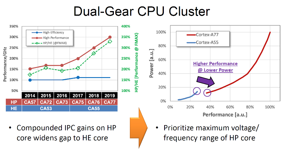
MediaTek’s initial response to a voltage droop was to provide a stored charge on die (capacitor) that can supply some instantaneous current, but this required valuable die area. As a result, it decided to move to clock stretching to save die space.
A big change for MediaTek was the use of a frequency locked loop (FLL) and not a phase locked loop (PLL). The FLL has dual clocks designed to never lose clocks cycles, but the design is less deterministic as it allows the oscillator to vary with voltage. With a FLL circuit, MediaTek was able to make a ~35mV improvement Vmin for about a 10% power savings. MediaTek also built a novel JTAG solution for the chip with a Gateway TAP for hierarchical access to test circuits.
The MediaTek chip also features WiFi 6 and support for 5G stand alone and non-stand-alone modes. The CPU complex is only 9.4 m2 and the A77 cores support up to 2.6 GHz clock speeds. The chip has an Arm Mali G-77 nine-core GPU.
TI automotive chip features ASIL-D support
The TI processor is designed for automotive applications. This chip is part of the Jacinto 7 SoC family. The design is a mix of Arm Cortex processors and TI’s own C71 DSP. For this design, TI created multiple isolated domains on the monolithic chip. With the domain isolation, parts of the chip can be ISO 26262 ASIL-D compliant for safety critical operations. Other parts of the chip will only require ASIL-B compliance.
The wakeup domain is ASIL D and has a dedicated Cortex-M processor for boot management, cryptographic acceleration, trusted execution environment, and secure storage.
The MCU domain is also ASIL-D and is isolated, with a Cortex-R processor. It supports communications with safety critical peripherals.
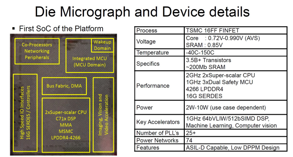
The main domain is ASIL-B and has Cortex-A processors and TI’s C71x DSP, plus a C66 DSP for audio processing and legacy support. The C71x DSP has a 64-bit, 16-issue VLIW architecture that can support 4240 integer MAC/cycle (8-bit). TI added many vision pre-processing functions for ADAS vision sensors that enhance the sensor data. There is also a depth and motion perception accelerator (DMPA) that estimates 2D object motion and builds a vector field between two images. This information can be used to estimate the potential for objects to cross the path of the vehicle.
IBM Z Series mainframes squeeze in more cores
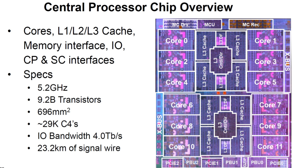
IBM’s venerable mainframe computers continue to move forward. The latest Z15 processor packs 12 cores capable of 5.2 GHz clock speeds with no thermal throttling, because IBM uses water cooling to handle the high power. While many other processors have moved to 7 nm, IBM instead stayed with the GlobalFoundries’ tried-and-true 14 nm process with embedded DRAM (eDRAM). Both IBM Power and Z series processors have relied on eDRAM to be able to put large caches on die, but this 14 nm GlobalFoundries is the end of the road for eDRAM scaling.
Despite being in the same process node as its predecessor, the Z15 designers squeezed in two additional CPU cores in the same die area plus 10% higher single-thread performance. Most of the work to shrink the cores was from tighter circuit designs. For additional die area savings, they removed voltage regulators off chip and redesigned the eDRAM to improve density.
In addition to the two extra CPU cores, the designers added in a cryptographic accelerator and sort/merge accelerator. The final chip was 696 mm2, which is about the same as its predecessor. Keeping the die size similar reduced the thermal and mechanical redesign work required.
Due to time constraints, each presentation could only touch on a few design aspects of these chips. Yet, it offers a glimpse of the incredibly complex nature of the design tradeoffs and tricks needed to squeeze out the maximum performance, for the lowest amount of power. It also demonstrates the shift in focus to architecture enhancements and advanced circuit design as the benefits of new process nodes decreases, especially relative to the cost.