Enabling advanced ICs with multiple patterning
Article By : Richard A. Gottscho
Advanced patterning techniques overlay multiple patterns of larger dimensions to achieve smaller and/or more tightly packed features.
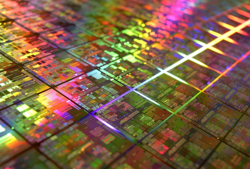
For decades, one of the major trends in electronics has been miniaturisation, which has helped pack in more functionality, extend battery life, and lower production costs per chip. Up until recently, the semiconductor industry has been able to meet consumer demands for smaller, more powerful products by scaling lithography capabilities to shrink integrated circuit (IC) feature dimensions. In conventional lithography, a wafer is coated with a light-sensitive material called photoresist, then light is streamed through a photomask (a pattern of transparent and opaque areas), causing only certain areas of the wafer to be exposed. In the case of positive photoresist, the exposed areas are subsequently etched away while the remaining areas are left intact, resulting in a set of features determined by the original photoresist pattern.
While this technique has been used successfully for many years, today’s advanced chip designs have smaller and denser features that require going beyond limits imposed by the wavelength of light used in conventional lithography. To create these chips, advanced patterning techniques overlay multiple patterns of larger dimensions to achieve smaller and/or more tightly packed features.
Multiple patterning 101
The most basic form of multiple patterning is double patterning—increasing feature density two-fold. One of the most common double patterning schemes is litho-etch-litho-etch (LELE), which involves two exposures and two etch steps. Using two distinct lithography steps allows for significant flexibility in design as each mask can be optimised independently. In this process, the complete photomask pattern is divided into two less feature-dense parts. The first pattern is transferred onto an underlying hardmask through lithography followed by etching, and then the process sequence is repeated for the second pattern. A key challenge with this technique is that the two patterns should be aligned perfectly but imperfections in overlay persist – nothing is perfect. Reducing overlay errors is a primary area of focus today. Otherwise, the resulting combined pattern can have significant relative displacement, leading to electrical yield issues.
Improving alignment: Spacer-based patterning
The self-aligned double patterning (SADP), or spacer-based technique, has been adopted in more aggressive product designs due to its effectiveness in reducing variation caused by mask-to-mask misalignment. With the simplest SADP approach, spacers are formed on the sidewalls of a pre-defined feature (a mandrel) through deposition and etch process steps. The mandrel is then removed by an additional etch step, leaving the spacers, which are subsequently used to define the desired final structures. Through this scheme, feature density is doubled since there are two spacers for each mandrel, and each feature is “registered” to the next by the original size of the mandrel.
SADP applications include the formation of fins in finFET technology, lines and spaces for interconnect levels, and bit line/word line features in memory devices. This technique replaces the second step of lithography in LELE double patterning with additional deposition and etch steps. The critical dimensions are created by spacer formation and mandrel removal rather than lithography, and strict process control for the deposition and etch steps is necessary to ensure proper feature spacing.
Multiple patterning driving miniaturisation
One advantage of the spacer-based technique is that it can theoretically double the pattern density indefinitely by repeating the spacer formation and pattern transfer steps. For instance, self-aligned quadruple patterning (SAQP) can achieve a half-pitch resolution of about 10 nm with 193 nm immersion lithography printing near the immersion limit of 40 nm half-pitch. Correspondingly, with such small feature dimensions, the control of process variability becomes more essential as more steps are added. Advanced processes that deliver atomic-scale control play a crucial role in enabling multiple patterning to create small and complex semiconductor devices.

Figure 1: The self-aligned spacer technique can double the pattern density indefinitely by repeating the spacer formation and pattern transfer steps.
Richard Gottscho, Ph.D., is executive VP, Global Products at Lam Research Corp.
Next: Resolve process variation challenges in multiple patterning »