Diamond chips oust saphhire for semicon ICs
Article By : R. Colin Johnson
Startup Akhan Semiconductor expects to announce a diamond semiconductor IC in a consumer product by next year, which promises to be faster, use less power, and thinner and lighter than silicon.
The semiconductor industry may soon be rolling out the red carpet for diamond chips. Akhan Semiconductor Inc. is licensing the diamond semiconductor process from the U.S. Energy Department's Argonne National Laboratory to realise the promise of diamond semiconductors that have been known to be faster, use less power, and thinner and lighter weight than silicon. The startup may be making significant headway towards realising this potential.
Akhan Semiconductor has a 200mm wafer fab in Gurnee, Ill. and expects to announce a diamond semiconductor IC in a consumer product at the Consumer Electronics Shows (CES) 2017.
Since before 2000, Argonne National Lab has been experimenting with diamond chemical vapour deposition (CVD), spinning off Advanced Diamond Technologies Inc. who partnered with Innovative Micro Technology to produce diamond microelectromechanical systems (MEMS) and inspiring diamond wafer specialists like SP3 Diamond Technologies to create the CVD equipment to deposit perfect crystalline diamond.
So far, however, the biggest successes for diamond have been in jewellery, abrasives and other industrial uses of man-made diamonds. Nevertheless, Argonne National Labs continued pursuing the dream of diamond semiconductors by finding a way to make diamond, a natural insulator, into a semiconductor and a conductor laying out the path to all diamond chips.
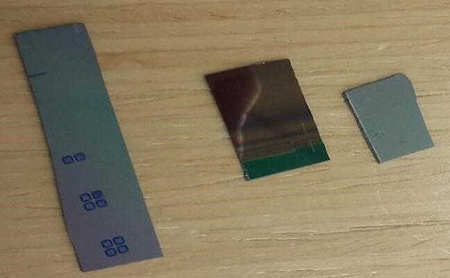
![[Diamond Chips 2 ]](/wp-content/uploads/sites/4/2020/04/EEIOL_2016MAY17_MFG_NT_06_01__1.jpg)
Figure 1: Samples of diamond on silicon from Akhan. (Source: EE Times)
The biggest problem that kept diamond from being commercialised, until now, has been the ease of making p-type transistors, but the difficulty of making n-types, a problem solved by founder and CEO of Akhan Semiconductor, Adam Kahn, who dubbed his process the Miraj Diamond Platform. With both p- and n-type devices, diamond complementary metal oxide semiconductors (CMOS) are now possible. Akhan Semiconductor hopes to roll out the world's first CMOS-compatible diamond semiconductors.
![[Adam Khan]](/wp-content/uploads/sites/4/2020/04/EEIOL_2016MAY17_MFG_NT_06_02.jpg)
__Figure 2:__ *Adam Khan, Akhan Semiconductor founder & CEO, showed samples to EE Times on May 3, 2016. (Source: EE Times).*
"We recently demonstrated CMOS-compatible diamond semiconductors, with both p-type and n-type devices, by successfully fabricating diamond PIN [abbreviation for a p-type, intrinsic, undoped, n-type junction] diodes with a million-times better performance than silicon and one-thousand-times thinner," Khan said.
Its secret was co-implanting phosphorous in p-type devices and co-doping barium and lithium into n-type devices, resulting in tunable electronics that achieve comparable performance in both types, thus enabling diamond CMOS. The company's first demonstrated device, however, was a diamond PIN diode that was a record-breaking 500nm thin. This type of performance is due to diamond being a super wide band-gap material, wider than even silicon carbide and gallium nitride.
"Thermal analysis showed that there were no hot spots on our PIN either, so there were no parasitic losses like with silicon PIN diodes," Khan noted.
Khan has also demonstrated 100GHz devices by virtue of the ultra-low resistance of diamond, which can be deposited on silicon, glass, sapphire or metal substrates. Those kind of speeds could revitalise the processor races, which have been idled at 5GHz for a decade. With silicon, 5GHz is the limit, since their high power consumption and thermal hot-spots turn devices into soup, but diamond has 22 times the thermal conductivity of silicon and five-times that of copper, Kahn claimed.
The company's ultimate goal is to revitalise the processor race with faster and faster clock rates, but for now they are concentrating on power electronics for industry, tunable optical military applications for countermeasures, and optical mobile consumer applications using diamond as the insulator and semiconductor, but still requiring indium tin oxide (ITO) for contacts (for now).
After banking some successful applications for angel investors and private equity firms who have provided Akahn's research and development capitol so far (to the tune of about $2.5 million). Akahn plans to announce Series A funding later this year, prompting them to come out of the closet at this time to attract a little attention about the possibilities that diamond semiconductors hold.
"We are not developing our mobile and consumer platform yet. For now our major application is power electronics that is more heat efficiency, but which works just like silicon devices, using the same lithograph, etching and metallisation steps, just adding the diamond deposition step," Kahn said.
But its ultimate goal is to take-the-heat-off (literally) of Big Data applications with ultra-cool-running processors. In fact, the high speeds capable of diamond CMOS is traded off against heat. In other words, data centres could cut their heat vastly, by running diamond processor at the same 5GHz of silicon, or could bump up their speed to the sub-terahertz range while consuming the same power as silicon.
![[diamond on silicon]](/wp-content/uploads/sites/4/2020/04/diamond_on_silicon.jpg)
__Figure 3:__ *Sample of diamond on silicon from Akhan Semiconductor, May 3, 2016. (Source: EE Times)*
"Heat is our major issue, half of big data energy today is wasted just keeping its silicon processors cool," Kahn added. "Diamond is next obvious step because it is much more energy efficient. It can also be deposited on glass and sapphire to make completely transparent electronics, for consumer applications, such as transparent mobile devices."
Extending Moore's Law?
Moore's Law will also be extended, yet again, according to Kahn, since the 100GHz demonstration chips it is showing now use design rules in the 100s of nanometres. That leaves almost a dozen generations of shrinkage before diamond faces the single-atom levels the silicon is facing circus 2025.
"Today we are focusing on power applications on 12in wafers, hoping to drive down the costs of production with higher volumes," Kahn stated. "Our power devices are moving into pilot production at our own fab, but we are using the fab-lite model, that is produce small- to medium-sized runs ourselves, then transferring our process to foundries when we ramp up into volume production."
Besides power devices, Akahn also claimed to have fledgling customers for diamond MEMS devices, specifically for capacitive switching arrays used to dynamically tune antenna in high-end smartphones.
![[Sample board with diamond heat sinks]](/wp-content/uploads/sites/4/2020/04/Sample_board_with_diamond_heat_sinks.jpg)
__Figure 4:__ *Sample board with diamond heat sinks (a chip can sit directly on top of a heat sink). (Source: EE Times)*
Next, besides mobile and data-centre processors, Akahn aims to enter the quantum computer field, but not using the nitrogen vacancy method, but rather using their own proprietary doping techniques they are keeping as a trade secret for now.