Better-Trained Talent Needed for India to Move up the Value Chain
Article By : Faisal Kawoosa
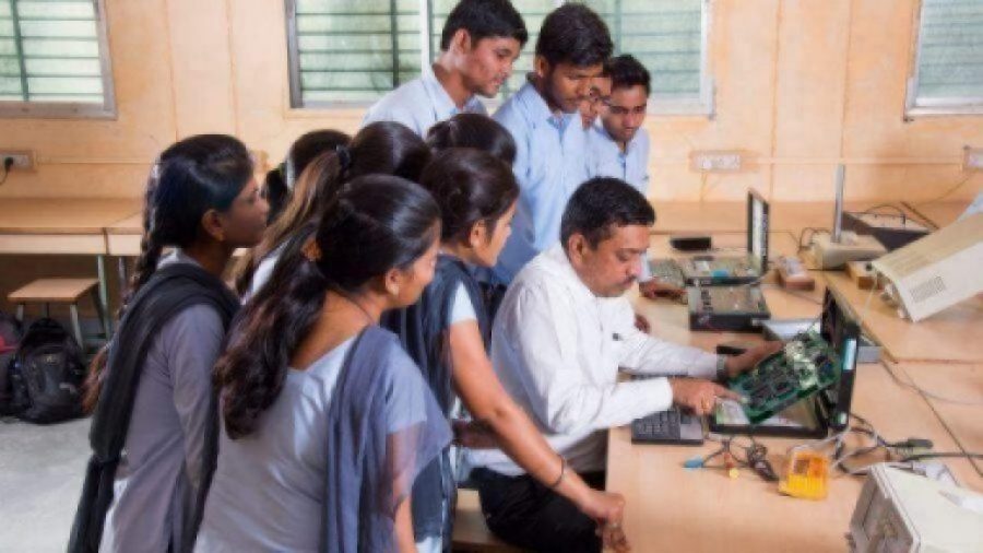
While India has a wealth of engineering talent, however, it could do a better job preparing its new engineers for evolving industry requirements.
India’s contribution to the global chip industry is undisputed. There is no major name in the chip industry that isn’t present in the country. Through its captive design centers as well as third-party offshore design-services suppliers, India contributes more than US$12 billion to the global semiconductor industry annually.
Because of strict confidentiality guidelines, we rarely come to know which chips have been significantly designed in India. But when the various aspects of VLSI design, verification, and embedded-software development are all taken into account, it’s fair to say that some of the most popular products of recent times can trace aspects of their design back to Indian engineers.
“There is probably no chip in the world [that] hasn’t been ‘touched’ by India in some way,” said P.V.G. Menon, president and CEO of VANN Consulting and former president of the India Electronics and Semiconductor Association.
What makes India so significant in the global chip supply chain? How have Bengaluru and adjoining cities become such prominent points on the chip industry map, perhaps next to Silicon Valley?
The not-so-secret sauce is the wealth of engineering talent available in India at very attractive price points relative to global labor costs. The starting salary of an R&D engineer in India ranges between US$1,500 and US$2,500 a month. That’s 40% to 50% of what one could expect in countries like the United States. It’s thus no surprise that the U.S. industry sources much of its chip-engineering talent in India, just as it has done for software. Rather than pay for high-cost homegrown talent, it makes economic sense for U.S. companies to recruit from India — and some Indian engineers aspire to move to countries like the U.S. at virtually any cost.
While India has a wealth of engineering talent, however, it could do a better job preparing its new engineers for evolving industry requirements. “Talent is not a problem at all,” said Parag Naik, CEO at Saankhya Labs, one of the few success stories in India’s semiconductor ecosystem. “At the mid- and senior levels, we have the people available abundantly. The challenge we face is at the entry level.”
This is a result of an archaic educational infrastructure at the country’s technical colleges. The top-tier tech institutes, namely the Indian Institutes of Technology (IITs) and some of the National Institutes of Technology (NITs), do a good job of ensuring academics are tightly aligned with industry requirements, but that is not the case elsewhere. In the National Policy on Electronics (NPE) 2012, the first comprehensive blueprint to foster the electronics and semiconductor industry in India, the government proposed a roadmap to address industry needs by awarding 2,500 doctorates in electronic-systems design and manufacturing annually by 2020. The plan hasn’t gone as expected, though not even those deeply connected with the industry have a clear grasp of the country’s progress toward its goal.
The aim of the Ph.D. target was to nurture more homegrown talent for product development and intellectual-property (IP) creation. This is critical for India, and most industry leaders in the country approve of the significance that the government has attached to it. “Our talent is one of the best in the chip industry globally,” said Jaswinder Ahuja, corporate vice president and managing director at Cadence Design Systems India. “What we now require is empowerment of talent to take higher-order skills in the chip industry for product development and IP creation.”
Clearly, both the government (with its policy intervention) and the industry (with its aspiration) understand the need for India to move up the hierarchy of skills in the chip industry if the country hopes to foster the emergence of high-tech startups in the domain. Where the country continues to fall short is in implementing the plan.
For instance, as part of the Ph.D. initiative, the government in 2014 sanctioned a US$56 million fund for a period of nine years that would be spent on stipends and other grants for full-time as well as part-time Ph.D. scholars in electronic-systems design and engineering services. But the actual awarding of funds to beneficiaries, particularly in electronic-systems design, is believed to have been negligible (again, there is no publicly available data on the program).
One reason for the poor uptake of this scheme is the dearth of relevant talent in sufficiently high numbers to exploit it. Even now, in the target year of 2020, India may not have a large-enough pool of potential students and professionals to yield 2,500 Ph.D.s annually in electronics. Indian universities’ Ph.D. programs have historically been oriented toward academic research rather than the practical research that could fuel a product- and IP-development ecosystem. The link between academics, product development, and the startup environment needs to be significantly strengthened, modeled along the lines of systems in the U.S., China, South Korea, and Taiwan.
India now has more than a decade of experience in chip design, a record that represents thousands of man-years of domain knowledge and practical experience. And the consumption of electronics in India is only increasing. The country needs products and solutions that could fire its ambition of a US$1 trillion digital economy by 2025, or 20% of the US$5 trillion GDP target that the government hopes to hit five years from now.
The potential is there for a strong ecosystem. The remaining weak leak is the creation of opportunities to help the country’s tech talent convert knowledge and experience into products and IP developed both in and for India.